
UV led lightbox
Trying to make my first pcb's I got pretty much annoyed by the fact that getting high quality pcb's suitable for smd was so much trouble. Experimenting with the direct transfer method brought me good results for simple boards, but not below a resolution of the printer. Neither my brother HL-5150D nor my HP color laserjet 2840 will give nice results with the direct transfer method below a resolution of 0,5 mm (metric size). Another approach was needed.
First tests
So the first home project was getting a UV exposure unit that will give consistent results. TL fluorescent lamps aren't consistent ie temperature drift, altered color when aging and sensitive to voltage changes in relation to light power output. So I decided for leds that are easier to handle.
For that I developed a KISS schematic that must serve a few purposes in a led design, as low as possible heat production over the current limiting resistors, have stable temperature light output and above all, limit the current to 20mA per led within the Voltage the array was designed for (12 .. 13.8 Volt), a voltage that is most of time available at the ham operators shack in sufficient power output.
Design
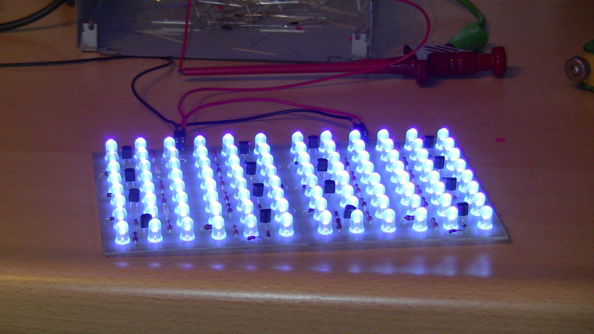 The actual design shines with simplicity and a bare minimum of components used.
The constant current source formed by a general purpose transistor (bc547), 2 diodes and 2 resistors is dimensioned for 40 mA per led array of 6 pieces, 2 pairs of 3 leds in serie.
The 2 diodes give a nice negative temperature feedback with the transistor when temperatures rise, hence limiting the total array at 320 mA (48 leds per section) at 12.5 Volts, even when much higher voltages are supplied or temperatures rise above 30 degrees Celsius.
This prevents burn out of the leds, even when 1 led fails and short out the circuit. The constant current circuit is capable of handling that too and still limits the current at approx. 20 mA per led.
About leds
The leds I used are 20 mA leds 3.2 Volts with a wavelength of 405 nanometer and a beam angle of 20 degrees. The beam angle is very important to prevent stray light. On the photo the leds look pale blue, but in reality this color is more purplish as you can see faintly by the glow around the leds at there top. The color shift is because my digital camera is not very sensitive to UV or near UV light (most digital camaras aren't).
Do not stare into the leds for a long time, you might encounter eye problems as welders sometimes encounter even if the leds seam not to be a strong light source, trust me, they are within there 20 degree angled beam. Getting them to light out evenly, the to be exposed PCB needs at least a distance of 8 – 10 cm or more, so that there beams slightly overlap. Getting the leds 'look' all into the same direction can be achieved with a small pipe wich is held over the led and fits snugly enough, to direct it while soldering the led. (Thanks to PE1BBC for the tip)
Getting the circuit into a nice case, is left to the you. You can go wild on that, by placing more array elements inside if you need a bigger surface to expose.
Below are the links to the actual pcb and component layout and the schematics file. The foto shows a eurocard (16 x 10 cm) with 2 complete sections, drawing each 320 mA at 12.5 Volts.
BOM per section
8 BC547 (b or c type)
8 ¼ watt metalfilm 1% resistor 18 ohm
8 ¼ watt resistor 2k2 ohm
16 diode 1n4148
48 UV leds 395 .. 405 nanometer 20 mA - 20 degree angled beam
1 single sided eurocard FR4
1 stitch power connector (2 lanes)
For a complete single sided eurocard of 16 x 10 cm (2 sections) you need twice the amount.